Press Release · Hanyang University
Hanyang University Researchers Gain Control Over Where Semiconductor Crystals First Form
Distributed by Phoenix Web Pros · Originally issued via PR Newswire
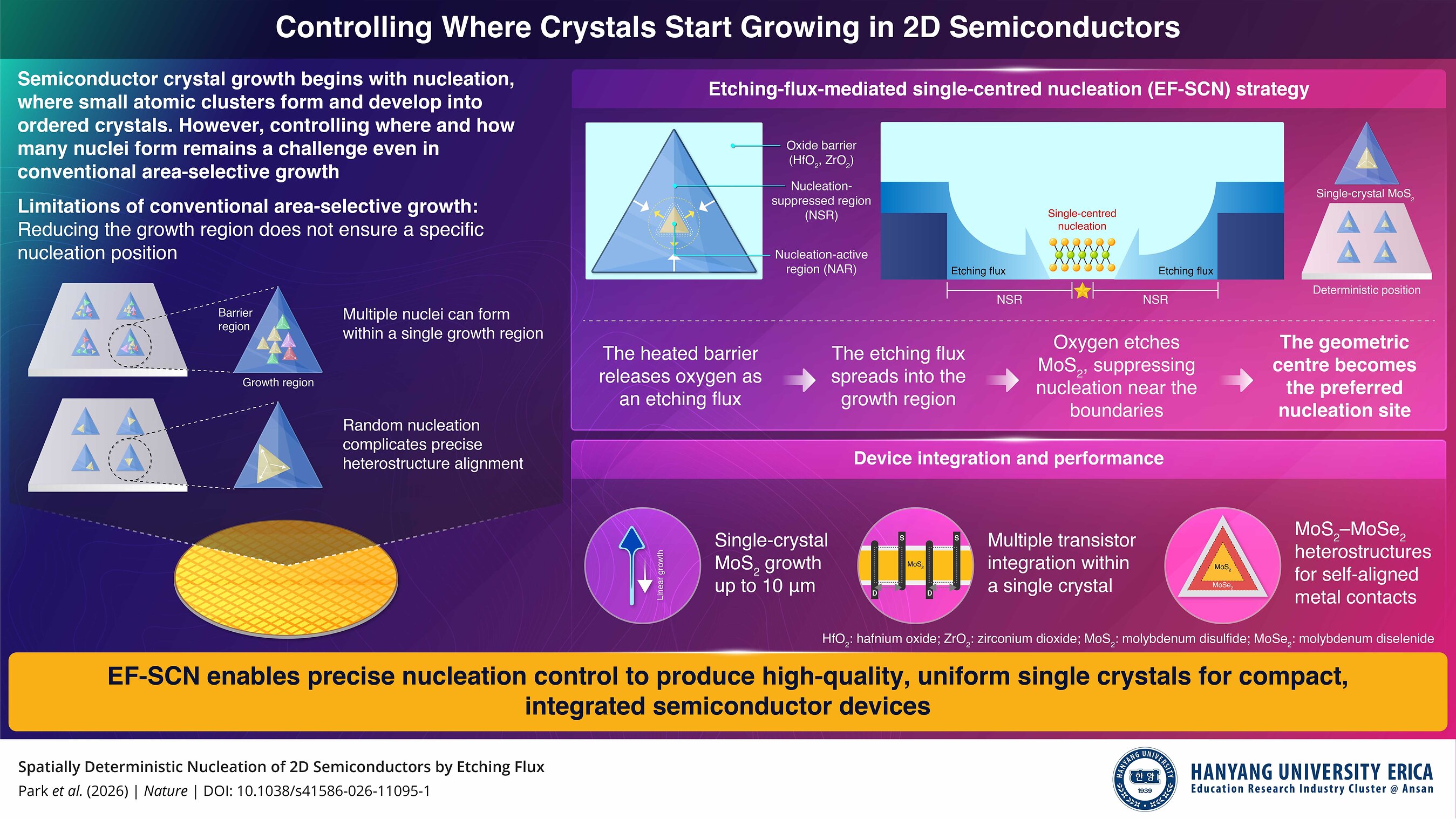
The method guides single crystals to begin growing in predefined central regions
GYEONGGI-DO, South Korea, Nov. 6, 2026 — Controlling where crystals begin to form is a challenge in manufacturing two-dimensional semiconductors. Researchers from Hanyang University and collaborating institutions developed a method called etching-flux-mediated single-centred nucleation to direct crystal formation at specific locations, achieving over 99% single-crystal growth across 400 sites.
In semiconductor manufacturing, nucleation, when crystals first begin to form, determines where and how they grow. This is particularly important for two-dimensional (2D) semiconductors, which are promising for next-generation electronics. However, conventional area-selective growth methods cannot reliably control where crystals begin forming within designated regions, making it difficult to produce large single crystals and precisely aligned structures for electronic devices.
In a study published in Volume 658 of Nature on October 7, 2026, Professor Woo-Hee Kim from Hanyang University, Republic of Korea, and colleagues introduced a method called etching-flux-mediated single-centred nucleation (EF-SCN), which uses oxygen released from an oxide barrier to control where crystals begin to form.
Using this approach, the researchers grew molybdenum disulfide (MoS2), a two-dimensional semiconductor, on patterned substrates using metal-organic chemical vapor deposition. They surrounded each designated growth region with a hafnium oxide (HfO2) barrier that releases oxygen when heated to 750°C. The oxygen etches the material near the pattern boundaries, suppressing nucleation in these areas and favoring the formation of a single crystal at the center. As growth continues, the crystal expands outwards to form a larger single-crystal region.
The researchers demonstrated consistent, centrally located nucleation across patterned arrays. As the crystals grew, they filled their designated regions, forming single-crystal domains several micrometers across.
The researchers also modified the method to allow crystal growth at lower temperatures by replacing HfO2 with zirconium dioxide, which has a lower crystallization temperature and serves as an alternative etching-flux barrier. This allowed them to grow uniform, centrally nucleated triangular single-crystal MoS₂ domains at temperatures as low as 430°C.
The researchers further investigated how growth conditions affect crystal formation. They found that the flow rate of diethyl sulfide, which supplies sulfur, primarily controls the number of nuclei that form. Too little can prevent nucleation, while too much can produce multiple crystals. The molybdenum precursor flow rate affects how far the crystals grow. By adjusting these conditions and the pattern dimensions, the researchers produced large crystals and line-shaped channels suitable for transistor integration.
The researchers produced crystals approximately 8 micrometers across and single-crystal films filling 10-micrometre growth regions. Across a 2-centimetre substrate, the method achieved a single-crystal yield exceeding 99%.
"To assess the electronic properties of these crystals, our team fabricated field-effect transistors using the MoS2 grown via our EF-SCN method," says Prof. Kim. The devices achieved a field-effect mobility of up to 117 cm2 V-1s-1. They integrated four transistors within a single crystal, with just 7.8% variation in electron mobility, demonstrating the potential to build denser electronic circuits with more consistent performance.
These findings establish EF-SCN as a method for controlling where crystals form, how they grow, and how they can be incorporated into electronic devices.
"This approach goes beyond conventional area-selective growth and enables highly reproducible single-crystal growth and provides a general framework for programming nucleation position, crystal geometry and subsequent device integration," says Prof. Kim.
Reference
Title of original paper: | Spatially deterministic nucleation of 2D semiconductors by etching flux |
Journal: | Nature |
DOI: |
Media Contact:
Jin-Mo An
82-31-400-4947
[email protected]
SOURCE Hanyang University
About Hanyang University ERICA
Website: https://www.hanyang.ac.kr/web/eng/erica-campus1